Measurement Process Optimization
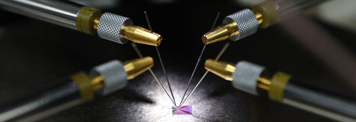
We verify and validate highly integrated circuits developed within our institute or provided by external partners within collaboration projects. Next to state-of-the-art electrical measurement equipment, we combine these with cryostats to enable device, circuit and system level characterization of the electronics at temperatures down to 10 Millikelvin, either stand-alone or in combination with semiconductor or superconducting qubits.
We investigate scalable thermal packaging solutions for electronics to qubit interconnect which allow placing the electronics in close vicinity to the qubits without degrading their performance due to local heating.
Contact


Infrastructure
- Chip verification and validation with state-of-the-art characterization equipment (low noise signal sources, arbitrary waveform generators, spectrum analyzers, network analyzers, oscilloscopes, noise characterization)
- Two closed cycle helium-4 cryostats for chip and single device characterization down to 5 Kelvin and up to 20 GHz
- Two dilution refrigerators with high cooling power (1.5mW @ 100mK) for chip performance measurements for qubit control and readout
- Wire-bonding (aluminum and gold) and flip-chip bonding
Lab Tools
Our lab tools aim for the optimization of measurement and post-silicon verification of our ICs. It includes a standardized interface to the measurement devices, administration of the measurement devices and the definition of measurement routines. For ICs, it includes a central storage for register and field definitions and the definition of routines for test cases.

Doctoral Researches - DR Projects
Meet the Team


Last Modified: 12.03.2025