Image Gallery
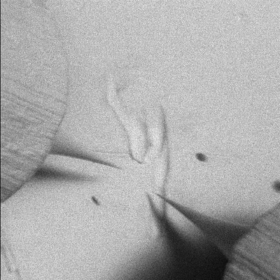
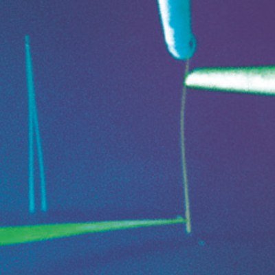
Movie of a tip approaching the surface (Note the
shadow of the tip on the surface, indicating the tip-sample distance)
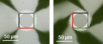
Four-tip measurements in a square
configuration for different rotation angles oft he tips

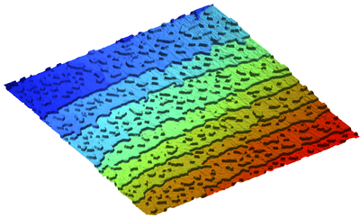
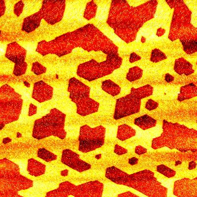
Potential measurements along a 2 μm long
wire segment
Multiprobe measurement on a freestanding
topological insulator nanowire
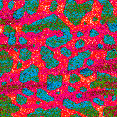
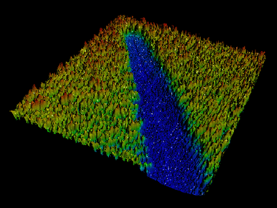
Potential map on a Si(111)-7x7 surface during
current flow from top to bottom
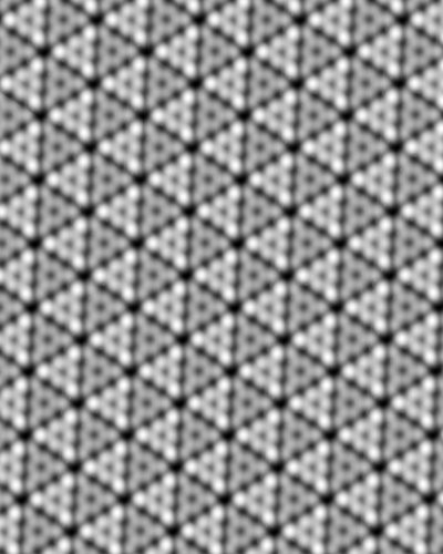
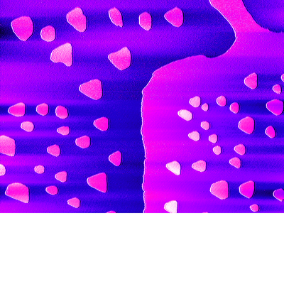
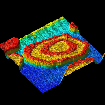
Potential map of a Si(111)/Ag-sqrt3 with
overlaid topography
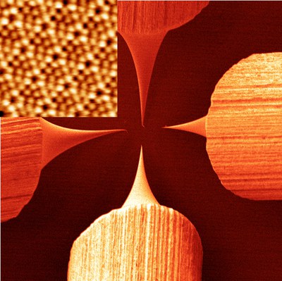
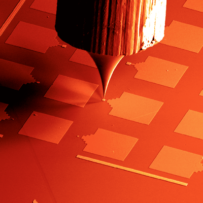
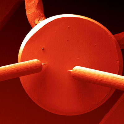
SEM view of four tips close to the surface
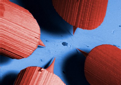
SEM view of four tips close to the surface
SEM view of four tips close to the surface.
Four-point measurement along a GaAs
Four tips close to a surface with silicide nanowires
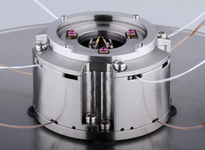
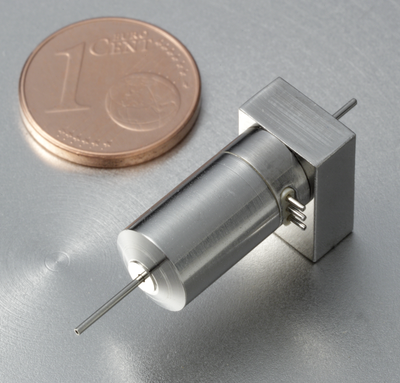
The ultra-compact Koala TetraProbe STM
integrates four independent STM units within a diameter of 50 mm
iezoelectric nanopositioner called
KoalaDrive
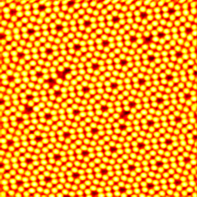
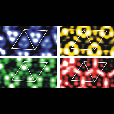
Si(7x7) surface with a domain of Bi sqrt 3
reconstruction
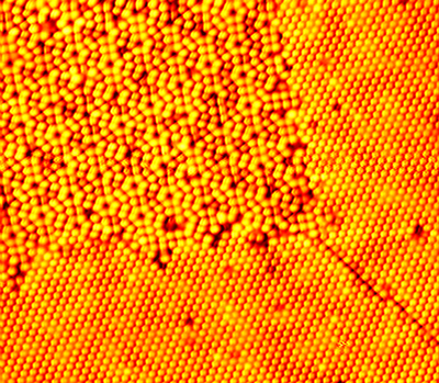
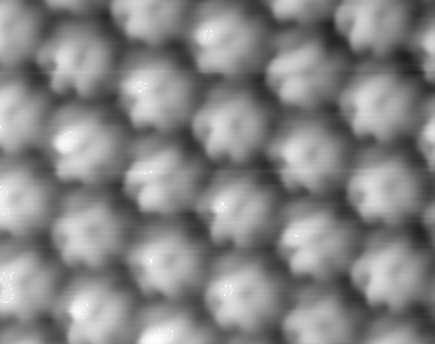
Si(7x7) surface
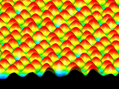
Rendered image of a Si(7x7) surface
Some surface reconstruction on Si(111)
Si(7x7) surface
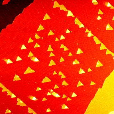
Bi on Si(111)
Bi on Si(111)
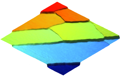
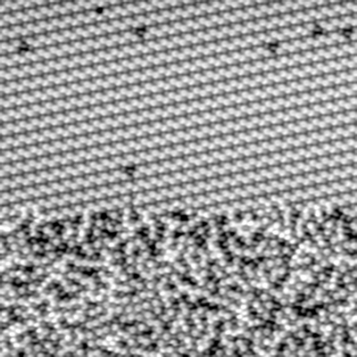
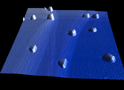
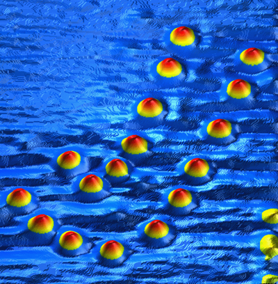
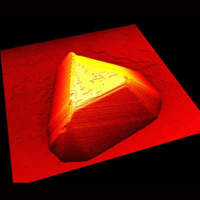
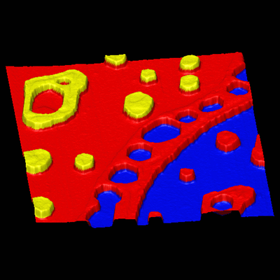
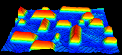
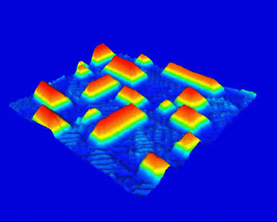
Si islands on Si(111)
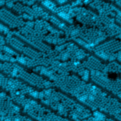
C_60 on Si(111)
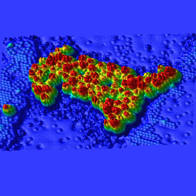
3D Ge islands on Si(111)
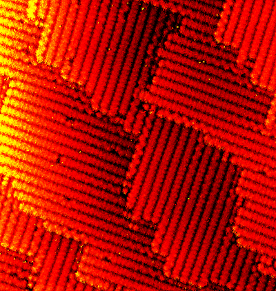
Bi reconstructions on Si(111

Bi reconstructions on Si(111)
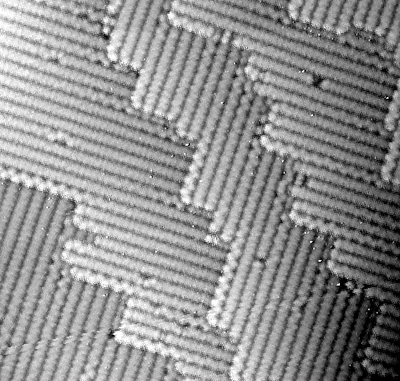
Si(100) reconstruction
Si(100) reconstruction
Si islands on Si(111)
Jülich logo written with CO molecules
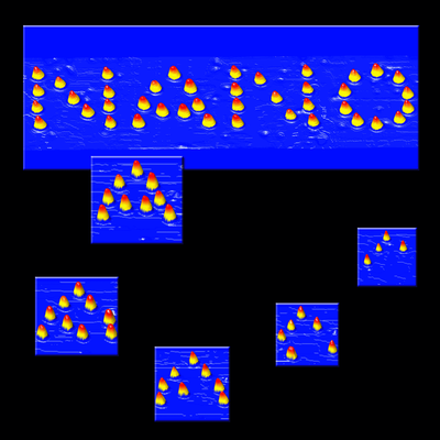
„Nano“ written with single C_60 molecules
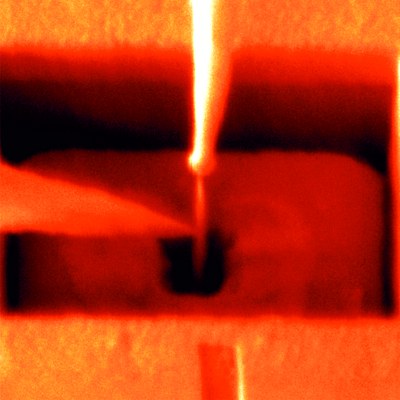
SEM image of a tip contacting a resonant tunneling diode
SEM image of a tip contacting a resonant tunneling diode (zoom)
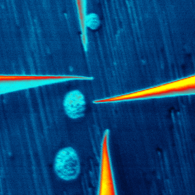
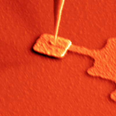
Two tips on a bead crystal
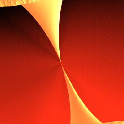
Two tips close to each other on a surface
3D Ge island on Si(111)
C_60 and Bi on Si(111)
Si(111) with Ge islands and Ge at the step edge, all covered by a Bi reconstruction
Si(111) dI/dV images

Si(111) with Ge islands, all covered by a Bi reconstruction
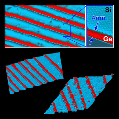
Si/Ge nanowires on Si(111). Si blue / Ge red
Shaddow image of a tip after in situ Bi evaporation
Si/Ge nanorings on Si(111). Si yellow / Ge red
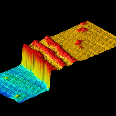
Si/Ge nanowires on Si(111). Si yellow / Ge red
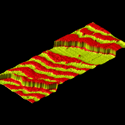
Si/Ge nanowires on Si(111). Si yellow / Ge red
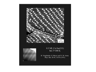
Co on Au(111): Nucleation of Co at the corners of the Au(111) herring bone reconstruction
Ge islands on Si(111)
Ge islands on Si(111)