Shadow Wall Epitaxie: Growth of Tomorrow
A team of dedicated researchers and material specialists at Forschungszentrum Jülich developed a chip manufacturing technology: the Shadow Wall Technique.
The Shadow Wall Technique is a selective orientation-dependent molecular beam epitaxial growth concept for the local definition of the explicit device areas. This enables for the all in-situ fabrication of fully independent complete products such as field-effect transistors (FETs), light-emitters and detectors.
This technique is considered innovative due to its integration of compound semiconductors with the leading edge CMOS technology. Its ability to tailor composition and doping profiles with an atomic distance precision is a game changer. Furthermore, it presents an etch-free implementation of hybrid devices, as well as a complete in-situ process flow.
The Shadow Wall Technique presents superior performance and high quality compound semiconductor devices. Another advantage of this technique is its scalable technology with further integration prospects as well as the drastic reduction of fabrication efforts and costs that it offers. Finally, the technique provudes rapid prototyping assistance of next generation technology products.
The constant innovation in chip manufacturing technology pushes the physical limitations and technological bottlenecks. The integration of new materials into semiconductor technology promises a major revolutionary impact on various applications.
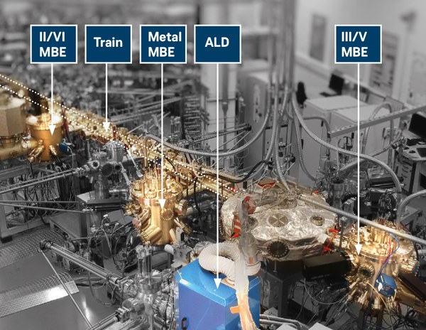
The innovative Shadow Wall Technique for Molecular Beam Epitaxy (MBE), allows the growth of various platforms of semiconductors with superior crystal quality. The prefabricated Shadow Walls confine the molecular beams to locally defined explicit device regions.
In combination with the deposition of metals and oxides, this technology allows the realization of various fully in-situ processed devices with low ohmic electrical contacts as well as gate terminals.

Shadow Wall technique explained by the researchers:
About the researchers:
We are a team of dedicated researchers and material spe-cialists at Forschungszentrum Jülich GmbH with the strong expertise in the epitaxial growth of compound semiconductors and nanofabrication.
PD. Dr. Alexander Pawlis
Head of Semiconductor Epitaxy and Quantum Optics Group & Scientific Head of the Nanocluster
Dr. Yurii Kutovyi
Scientist & Expert on Micro/Nanofabrication of Semiconductor Devices

Dr. Nils von den Driesch
Scientist & Expert on Semiconductor Growth and Analysis
Contact:
Email: a.pawlis@fz-juelich.de
Tel: +49 2461 61-2077
Forschungszentrum Jülich
Peter Grünberg Institute (PGI-9) Wilhelm-Johnen-Straße
52428 Jülich, Germany