Wave packet motion through a nanoscale contact.
Electrons move in nanoscale devices as matter waves. It requires a quantum mechanical treatment. In allmost all experimental setups the electrons are bound in a plane between two material blocks of different chemical composition,
e.g. Indium-Phosphid and Indium-Gallium-Arsenid. The electron motion is two dimensional and is easily visualised in a two dimensional contourplot of the density. The figure below shows the passage of an electron wavepacket through a ringshaped contact in an InP/InGaAs heterostructure as an animated picture. The time scale is determined by the size of the contact - 800nm ring diameter, 85nm width of the ring arms - and the effective mass of the electrons in the material - 0.037 times the value for an electron in free space. With these parameters the duration of the wave packet motion in the figure below is 30psec.
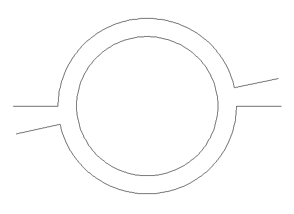
The example chosen here shows clearly the phenomenon of wave-packet splitting. After a first strong reflection when the wave hits the wall of the ring at the entrance to the right only part of the wave moves through the arms into the exit region. But again not the whole wave leaves the ring, part of it travels back and leaves the entrance roughly 12psec after the first reflection.
(A.Bringer)