Organic and Hybrid Solar Cells
About
Printable semiconductors allow the production of solar cells at low cost on flexible substrates. The use of semiconductors with different absorption bands (i.e. different band gaps) allows the production of multi-junction solar cells, which thus enable higher efficiencies than the current technology ofcrysalline silicon single-junction solar cells. The examined material classes for printable semiconductors are mainly organic semiconductors (e.g. polymers and small molecules) as well as certain inorganic semiconductors, such as the class of halide perovskites.
Research Topics
Technology development, Characterization, and Simulation of Solar Cells


Printable Solar Cells
The currently dominant solar cell technology is based on crystalline silicon (Si). This technology has the advantage of high stability (> 20 years) and high efficiency of 26% and the costs that have decreased significantly over the years due to mass production. Disadvantages of silicon solar cells are the relatively high energy consumption during production, the relatively high layer thicknesses that are necessary because of the indirect band gap of silicon, and the limitation of the efficiency to a maximum of about 29%. Higher efficiencies are only possible with multi-junction solar cells based on the use of more than one absorbing semiconductor material.
One focus of photovoltaic materials research is therefore the development of materials that circumvent these limitations. Printable semiconductors allow the production of solar cells at low cost on flexible substrates. The use of semiconductors with different absorption bands (i.e. different band gaps) allows the production of multi-junction solar cells, which thus enable higher efficiencies than single-junction solar cells. The examined material classes for printable semiconductors are mainly organic semiconductors (e.g. polymers and small molecules) as well as certain inorganic semiconductors, such as the class of halide perovskites.
Further information on our research and infrastructure
Perovskite Solar Cells
For halide perovskites, precursor molecules are applied from the liquid phase to a substrate. The layer is then briefly tempered (at 100 to 200°C) so that the solvents evaporate and a crystal can form, which consists of the elements in the precursor molecules. In the process, thin polycrystalline layers are formed, some of which have optical and electronic properties that are better than those of Si single crystals that are produced from a Si melt (melting point of Si: 1410 ° C). Perovskite solar cells have achieved efficiencies of> 25% in a relatively short time (see https://emerging-pv.org/), and tandem solar cells made from halide perovskites and silicon have surpassed the 30% efficiency threshold.
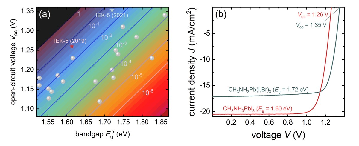
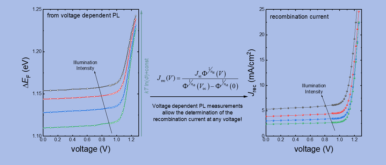
One of the key properties of certain halide perovskites are their comparably long carrier lifetimes. These long lifetimes in combination with the high absorption coefficients lead to high photoluminescence efficiencies, which makes the materials interesting for both light-emitting and photovoltaic applications. The luminescence quantum efficiency correlates directly with the open circuit voltage. In the limiting case of purely radiative recombination (luminescence quantum efficiency = 1) one would obtain the highest possible open-circuit voltage for a given band gap (black line in Figure 1 a). For every magnitude of reduction in luminescence quantum efficiency, the open circuit voltage drops by about 60 mV [3]. In reality, every solar cell has a substantial proportion of non-radiative recombination, so that the luminescence quantum efficiency of the solar cell is significantly less than 1.
With the aim of achieving high open-circuit voltages, scientists in the group are developing processes for absorber materials and contact layers with extremely low, non-radiative recombination losses. In addition, a whole range of measurement methods (luminescence, photoelectron spectroscopy, electrical measurements) are used to investigate the recombination in the materials and at the interfaces. At the beginning of 2019 a paper was published with an open circuit voltage of 1.26 V [1]. This value is only 60 mV below the thermodynamic limit of 1.32 V (for purely radiative recombination) and is therefore the highest open circuit voltage that was achieved in this material system relative to the band gap (see Figure 1 ). The cells have luminescence quantum yields of 5 to 10%, which is also the highest value achieved so far for perovskite solar cells. The result shows that it is possible to contact the perovskite layers in such a way that the contacts no longer cause any noteworthy recombination losses. The missing 60mV to the radiant limit is largely due to optical losses (parasitic absorption), which is a situation that otherwise only exists in GaAs solar cells with extremely complex manufacturing.
These results are of particular relevance for the development of highly efficient tandem solar cells. These are based on the basic idea that photons with higher energies (visible light) are absorbed in a semiconductor with a higher band gap and their energy is extracted there as electrical current at a higher voltage (i.e. energy per charge carrier). Photons with lower energies (red and near-infrared radiation) are absorbed in a second semiconductor with a lower band gap and result in a lower voltage. In order to produce efficient tandem cells, it is crucial that the cell with the high band gap (e.g. a perovskite solar cell) extracts the electrons at the highest possible voltage.
Organic Solar Cells
In order to reduce the cost of solar cells, manufacturing techniques are required that allow the fast fabrication of thin films at low temperatures. A high speed means that the (expensive) machines are used efficiently while the low thickness of the films reduces the amount of required raw material and the low temperatures save energy. Printing of solar cells fulfills all these requirements but it requires specific materials that can be printed from solution. One of the most thoroughly studied family of solution-processable semiconductors are organic materials. Organic semiconductors are e.g. conjugated polymers but also small molecules like fullerenes (e.g. derivatives of C60 or C70). Many of those organic semiconductors are very efficient light absorbers and allow solution processing without the requirement for expensive equipment or explosive solvents like hydrazine. However, the challenge is to make highly efficient solar cells from organic semiconductors.
Organic semiconductors typically have rather small relative permittivities which implies that the Coulomb attraction between two differently charged carriers (like electrons and holes) are much stronger than in an inorganic semiconductor. Therefore, an absorbed photon does not directly create an electron-hole pair but initially a strongly bound Frenkel exciton (see Figure 2 a). This exciton has a binding energy much larger than the thermal energy kT at room temperature (~ 25 meV). Therefore, a trick is required to split the exciton. This trick is a type II heterojunction see e.g. http://en.wikipedia.org/wiki/File:Heterojunction_types.png) as shown in Figure 2 a. A type II heterojunction has discontinuities of conduction and valence band with the same sign. Figure 2 a shows that the energy levels of the left molecule are always higher than that of the right molecule. Therefore, it is energetically favorable for the bound electron to hop from the left to the right molecule. Because of the discontinuity in the bands at the interface it is very unlikely that the electron overcomes the barrier to return to the left molecule. For the hole it is more favorable to stay on the left molecule (for holes the energy axis is inverted) which means that the type II heterojunction allows the splitting of the Frenkel exciton into an electron and a hole on two separate molecules.
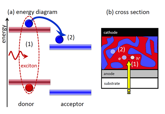
Exciton diffusion lengths are typically about 10 nm while the absorber layer thickness needs to be at least around 100 nm to absorb a substantial part of the light. This means that two thin layers of molecule A and molecule B on top of each other would not be sufficient for high efficiency solar cells. If the layers are very thin, the solar cell would be essentially transparent. If the layers were thick, the solar cell would absorb the light but only a small fraction of it would be absorbed within an exciton diffusion length of the interface and therefore only few electrons and holes would be created. In both cases the photocurrent would be relatively small.
The solution for this dilemma is shown schematically in Figure 2 b. In a so-called bulk heterojunction, the two molecules are mixed such that (ideally) each point in the volume is within about 10 nm to the next interface. In addition, one needs to make sure that there are percolating pathways such that electrons and holes can be transported to their respective contacts. The bulk heterojunction (BHJ) concept is a source of various scientific questions dealing e.g. with the ideal microstructure of a BHJ or the ideal energy level alignment at the interfaces.
The efficiency of organic solar cells has improved significantly in recent years through the use of new types of acceptor molecules (non-fullerene acceptors, NFAs), so that the efficiency now reaches values > 19% that were until recently only achievable using inorganic solar cells. A major focus of the group is the fabrication and characterization of efficient organic solar cells with novel NFAs, the improvement of the open circuit voltage [4], the use of ternary compositions and the optimization of the absorption in narrow energy ranges, e.g. for use in tandem cells.
In addition, the group is working on new measurement methods for determining electronic properties such as charge carrier lifetimes and mobilities as well as on the fundamental understanding of device physics [6]. In addition, the group deals with the fabrication and optimization of organic solar cells for indoor applications for the Internet of Things [7].
Highlights


References
[1] Liu, Z., Krückemeier, L., Krogmeier, B., Klingebiel, B., Márquez, J. A., Levcenko, S., . . . Kirchartz, T. (2019). Open-Circuit Voltages Exceeding 1.26 V in Planar Methylammonium Lead Iodide Perovskite Solar Cells. ACS Energy Letters, 4(1), 110-117. doi:https://doi.org/10.1021/acsenergylett.8b01906
[2] Liu, Z., Siekmann, J., Klingebiel, B., Rau, U., & Kirchartz, T. (2021). Interface Optimization via Fullerene Blends Enables Open-Circuit Voltages of 1.35 V in CH3NH3Pb(I0.8Br0.2)3 Solar Cells. Advanced Energy Materials, 11(16), 2003386. doi:https://doi.org/10.1002/aenm.202003386
[3] Krückemeier, L., Rau, U., Stolterfoht, M., & Kirchartz, T. (2020). How to Report Record Open-Circuit Voltages in Lead-Halide Perovskite Solar Cells. Advanced Energy Materials, 10(1), 1902573. doi:https://doi.org/10.1002/aenm.201902573
[4] Chen, X.-K., Qian, D., Wang, Y., Kirchartz, T., Tress, W., Yao, H., . . . Gao, F. (2021). A unified description of non-radiative voltage losses in organic solar cells. Nature Energy, 6(8), 799-806. doi:https://doi.org/10.1038/s41560-021-00843-4
[5] Baran, D., Gasparini, N., Wadsworth, A., Tan, C. H., Wehbe, N., Song, X., . . . McCulloch, I. (2018). Robust nonfullerene solar cells approaching unity external quantum efficiency enabled by suppression of geminate recombination. Nature Communications, 9(1), 2059. doi:https://doi.org/10.1038/s41467-018-04502-3
[6] Hartnagel, P., & Kirchartz, T. (2020). Understanding the Light-Intensity Dependence of the Short-Circuit Current of Organic Solar Cells. Advanced Theory and Simulations, 3(10), 2000116. doi:https://doi.org/10.1002/adts.202000116
[7] Lübke, D., Hartnagel, P., Angona, J., & Kirchartz, T. (2021). Comparing and Quantifying Indoor Performance of Organic Solar Cells. Advanced Energy Materials, 11(34), 2101474. doi:https://doi.org/10.1002/aenm.202101474
Last Modified: 05.11.2024