High-resolution Electron Microscopy
Microstructural features on different length scales from sub-millimeter down to the atomistic structure impact materials properties. To cover the large range of length scales we use Scanning- and Transmission Electron Microscopy (SEM and (S)TEM), which in combination with the spectroscopic methods Energy dispersive X-ray Spectroscopy and Electron Energy Loss Spectroscopy (EELS) give insight into local chemistry. Electron Diffraction in the SEM and TEM (also 4D-STEM) provides insight into present crystallographic phases and orientations. Focused Ion Beam (FIB) allows to prepare site specific samples of microstructural features for more detailed studies down to atomistic structure in the TEM.
Our research interests are the influence of microstructure as well as crystallographic structure of materials, interfaces, and components of materials used for energy storage and conversion on their electrochemical performance.
For the sub-mm down to the nm scale we use scanning electron microscopy (SEM) imaging in combination with Energy dispersive X-ray Spectroscopy (EDS) and Electron BackScatter Diffraction (EBSD) to analyse local chemistry and crystal orientation, which provide insights into phase formation/segregation during synthesis and operation.
Focused Ion Beam (FIB) is used to perform such analysis in three dimensions by subsequentially cutting and imaging. From reconstructed sample volumes, quantitative distribution of phases, interfaces, triple phase boundary (TPB) and phase specific surfaces areas are retrieved, being important for the activity in porous electrodes for Solid Oxide Fuel/Electrolyzer Cells (SOFC/SOEC). Another application of FIB is the site-specific preparation of lamellas for TEM.
FIB-Tomography and STEM-EDS/EELS analysis of spindle like LiTi2(PO4)3 particle, which showed an improved cycling behaviour, showed that even minor phases such as TiO2 (anatase) nanoparticles can play a role, if they form a three dimensionally connected network. 1 The crystallographic structure for all phases could be shown by high-resolution images.
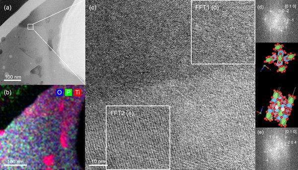
Based on high-resolution TEM imaging we provide a structural model of a grain boundary in Li1.3Al0.3Ti1.7(PO4)3 solid electrolyte for Li-Ion Batteries. 2, 3 Molecular dynamic simulations revealed that the conductivity across such an interface is almost comparable to that of bulk grains. The grain boundary conductivity observed in macroscopic experiments, which is three orders of magnitude lower than bulk conductivity, therefore must be attributed to other effects, such as crack formation at grain boundaries. 3
For the perovskite La(1-δ)FeO3, which is a catalyst for air electrodes in SOECs/SOFCs, EELS, EDS, HRSTEM and SEM investigations show that no La-deficient La(1-δ)FeO3 is formed during the solid state synthesis. No change of the Fe valence state could be proved by EELS, instead Fe2O3 is observed as secondary phase, in agreement with ab-initio calculations. 4
In-situ (HR)TEM and electron diffraction of electro spun polyacrylonitrile (PAN) derived carbon fibres show, how the carbon structure changes from amorphous to more turbostratic with increasing temperature, which explains the increasing electrical conductivity of such fibres carbonized at 800°C and above. 5, 6
Such carbon fibres can also be used as 3D-structured current collector matrix material for zero excess Li-Ion batteries. Li-deposition can be influenced not only by electrical conductivity but also lithiophilic–lithiophobic components. For sample series carbonized at different temperatures, STEM-EDS shows how Cu (lithiophobic) and Ag (lithiophilic) nanoparticles form in the fibres and how their size and distribution changes with carbonization temperature. The best cycling stability is observed for the sample carbonized at 700°C, which is explained by an optimum balance of electrical conductivity and lithiophilic–lithiophobic gradient. 7
Contact


Last Modified: 26.02.2025