Neuron-device interfaces
3D- & Nano-Structures
While microelectrode arrays (MEAs) offer a range of advantages such as their non-invasive nature, the ability to interact with cellular networks over extended times and at multiple sites with excellent temporal and spatial resolution, conventionally with the cost of signal quality. An approach for the improvement of the recording capabilities of MEA-based devices is to engineer the cell-electrode interface with the introduction of 3D structures. High aspect ratio 3D nanostructures and engineered surface patterns and nano cavities allow for unique biologically driven events to improve the cell-electrode coupling, providing high signal quality and allowing access to previously unattainable signals.

3D Structures

3D structures improve the cell-electrode coupling by inducing protein expression causing engulfment-like cellular behavior, thus increasing the cell-electrode contact. In our group, we investigate various different three-dimensional designs, e.g. cylindrical pillars, straws, mushroom-like pillars, and hollow mushroom all on a micro or nanoscale. We employ electron-beam lithography to define patterns that allow for the fabrication of these metallic 3D structures via electrodeposition, including developing a process that enables the galvanic deposition of individual 3D nanoelectrodes. These lithographic techniques combined with nanoscale additive manufacturing (3D printing) give us access to explore and utilize compound designs and various structures on a single chip.
The formation of a tight cell-electrode contact is a prerequisite for a high sealing resistance and high signal to noise ratio, we aim to understand the geometric and material conditions that facilitate a tight and stable interface. Employing HL 1 cells as a model system, we utilize focused ion beam sectioning for the investigation of the interface between cell and electrode. By gathering information about the cellular response to the nanostructures, we can better engineer electrodes for high quality cell-chip coupling.
Nanocavities

Introducing cavities on microelectrode arrays poses one way to address shortcomings in standard planar MEA systems. Specfically, they exhibit decreased noise due to comparatively large sensor areas while maintaining the high spatial resolution of µm-scale electrodes. Furthermore, a high sealing resistance is formed by cells covering the electrodes, decreasing signal loss while improving spatial resolution.
The nanocavites themselves are nanometer scale gaps between the microelectrode-array's (MEA) sensor material and its passivation layer.
A thin sacrificial chromium layer is evaporated on top of the gold or platiunum electrodes. This layer is only accessible through the electrode apertures. It is subsequently etched to produce the cavities.
Cultured cells adhering on the chip surface are suspended over the electrode openings, forming a tight seal.
With promising results obtained in electrochemical measurements, our work focuses on quantification, optimization and modification of the cell-cavity/electrode interface to achieve ideal signal coupling.
Characterizing the cell device interface
Structural information about the cell device interface is crucial for designing better sensing and stimulation devices and better implants. In particular, understanding the cellular interaction with surface topography and chemistry is imperative. To investigate the cell membrane conformation on a substrate, one requires techniques that have nanometer resolution in both, the lateral and axial directions relative to the cell-substrate-interface-normal and which ideally work in situ. For this purpose, we employ Surface Plasmon Resonance Microscopy (SPRM), Refractive Index Microscopy (RIM) and Scanning Electron Microscopy (SEM). For SEM imaging, a Critical Point Drying (CPD) and a resin embedding based preparations technique have been developed.

Ultra-thin resin embedding method for investigating cell surface interface
Our resin embedding approach allows to remove resin excess on the sample before full polymerization and preserves the cellular volume as well as small cellular features. The use of staining agents like uranyl acetate or osmium tetroxide allows for high contrast images (see Figure 1). In this way, all the morphological information of individual cells in contact with structured surfaces can be investigated in detail using Scanning Electron Microscopy (SEM). The imaging of ultra-thin FIB-sectioned, resin embedded cells is particularly relevant for the analysis of thin and fragile cellular compartments and the visualization of the actual interface between cell membrane and devices. Furthermore, using our resin method, it is possible to investigate low and high aspect ratio 3D nanostructure–cell interactions.
Investigation of the cell-chip interface using Surface Plasmon Resonance (SPR) Microscopy
Surface Plasmon Resonance Microscopy (SPRM) and Refractive Index Microscopy (RIM) are two label-free methods that we use to study the interface between cells and flat substrates. In case of SPRM, a cell-substrate distance can be measured with a sub-nanometer sensitivity. While in an SPRM measurement the data analysis also allows for the extraction of the intracellular refractive index (RI), the RIM mode of the same setup allows us to measure the intracellular RI with an even higher sensitivity (0.001 RIU) and to determine a samples birefringence [1].
SPRM is an imaging method based on the excitation of electron oscillations (Surface Plasmons [2]) at the surface of a metal layer. The energy of the excited Surface Plasmons depends on the dielectric constants within the metal layer’s environment [3]. Thus, if living cells attach to a metallic surface, the Plasmon excitation energy changes. Even if there is a coating in between the metallic surface and our cells, we can measure this change in excitation energy and hence use SPRM to investigate the cell-substrate distance in vitro [4].
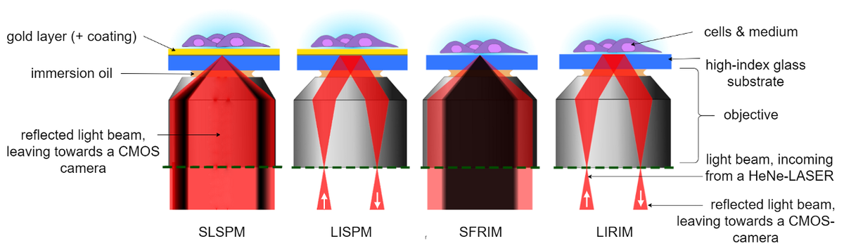
Having different sample illumination schemes, the SPRM- and RIM- modes can be further subdivided into two working modes, each (see Figure 2). As widefield imaging modes, our setup has a Lens-Imaging Surface Plasmon Microscopy (LISPM) and a Lens-Imaging Refractive Index Microscopy (LIRIM) mode, allowing for a sample-observation in real-time. For the extraction of quantitative information, however, our setup employs a Scanning-Localized Surface Plasmon Microscopy (SLSPM) or a Scanning-Focused Refractive Index Microscopy (SFRIM) mode.
While the lateral resolution of the LISPM is limited by the propagation length of the Surface Plasmons (several µm, depending on wavelength, type of metal and surface roughness [5]), the use of radially polarized light in the SLSPM mode allows us to generate localized Surface Plasmons with which we bypass this limitation [6].
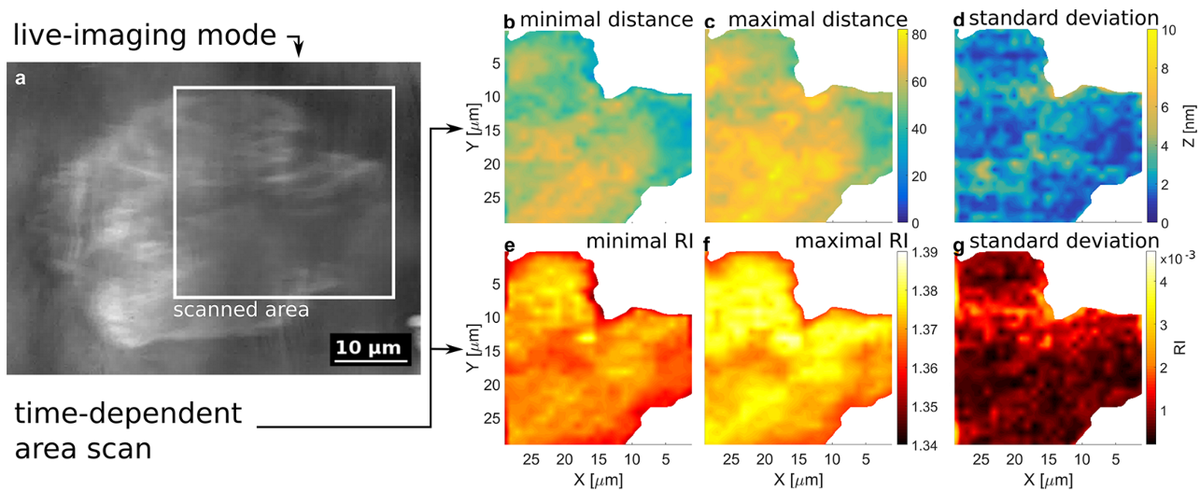
One of the applications of this setup is the comparison of cell adhesion for different substrate-coatings like lipid- or protein-coatings to improve electronic cell-chip interfaces. As these microscopy techniques are non-invasive and do not involve any toxic fluorescent dyes, they can be used in long-time experiments (see Figure 3).
[1] Hossein Hassani, 'From surface plasmon microscopy to refractive index microscopy: Label-free measurement of cell-substrate distance and intracellular refractive index' (doctoral thesis, RWTH Aachen University, 2021)
[2] Raether, H., 1988. Surface plasmons on smooth surfaces. In Surface plasmons on smooth and rough surfaces and on gratings (pp. 4-39). Springer, Berlin, Heidelberg.
[3] Somekh, M.G., Liu, S., Velinov, T.S. and See, C.W., 2000. High-resolution scanning surface-plasmon microscopy. Applied optics, 39(34), pp.6279-6287.
[4] Kreysing, E., Hassani, H., Hampe, N. and Offenhäusser, A., 2018. Nanometer-Resolved Mapping of Cell–Substrate Distances of Contracting Cardiomyocytes Using Surface Plasmon Resonance Microscopy. ACS nano, 12(9), pp.8934-8942.
[5] Kolomenski, A., Kolomenskii, A., Noel, J., Peng, S. and Schuessler, H., 2009. Propagation length of surface plasmons in a metal film with roughness. Applied optics, 48(30), pp.5683-5691.
[6] Watanabe, K., Horiguchi, N. and Kano, H., 2007. Optimized measurement probe of the localized surface plasmon microscope by using radially polarized illumination. Applied optics, 46(22), pp.4985-4990.
CONTACT:
Prof. Dr. Andreas Offenhäusser
Tel.: +49-2461-61-2330
e-mail: a.offenhaeusser@fz-juelich.de