Breakthrough in Photoemission Spectroscopy Allows Electronic Investigations Inside Crystals
The physical properties of solid substances are based on electronic states inside the materials. Now, an international team of researchers with the involvement of Jülich scientists has succeeded in studying these states in previously unimagined depths. The results have been published as an advance online publication by Nature Materials (doi:10.1038/nmat3089). In the "News and Views" commentary, the method is predicted to have a considerable potential for materials research.
For their measurements, the researchers from Germany, the USA, and Japan used the established method of angle-resolved photoemission spectroscopy. However, they used with a light source that was 100-times stronger than usual. This type of light is produced at a mere handful of scientific facilities throughout the world, in Germany, for instance, at the PETRA III storage ring in Hamburg. The team used SPring-8 in Japan, which is currently the world's most powerful synchrotron radiation facility in the hard X-ray range.
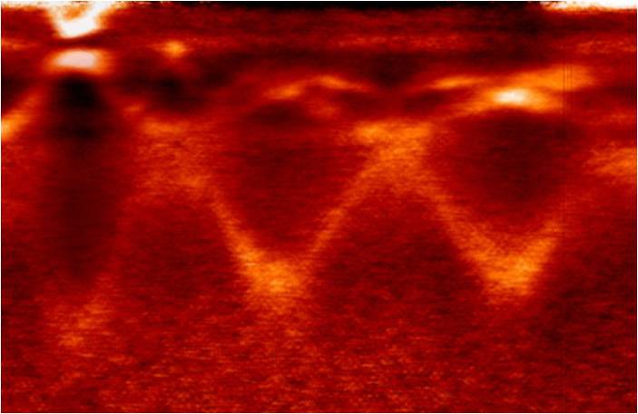
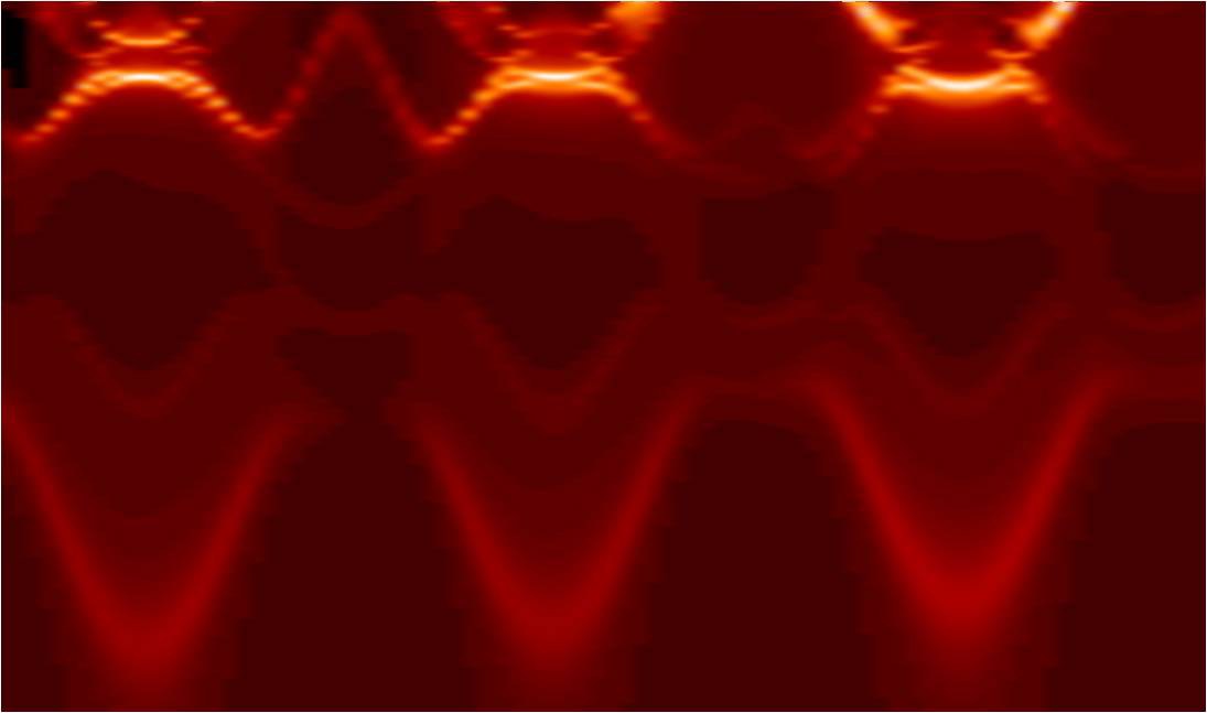
Photoemission spectroscopy has been used since the 1970s and is based on the photoelectric effect first theoretically described by Albert Einstein in 1905. Scientists use the method to irradiate samples with light, which causes electrons to become detached from the material. The distribution of angles and energy from the escaping electrons reveals information on the electronic states of the sample, for instance, the position and movement of electrons, band structures, or magnetic properties.
However, this had previously only been achieved for the first approximately five to ten atomic layers at the surfaces. From deeper layers, too few electrons reached the detectors of the measuring instruments. The scientists have now succeeded in achieving a view inside tungsten and arsenide over ten times deeper thanks to the especially brilliant light with high energies of up to six kiloelectron volts, an improved electron spectrometer, and cleverly selected sample material.
The participating scientists at SPring-8 adjusted the light source to allow a maximum number of photons to reach the sample on the smallest possible area. Experimental physicists from Jülich, Erlangen, Mainz, and Berkeley, optimized the spectrometer used and studied sample materials with low lattice vibrations in order to obtain the most detailed results possible. Theoretical physicists from Munich and Davis developed models that can be used to interpret the measurement results.
Probing bulk electronic structure with hard X-ray angle-resolved photoemission, A.X. Gray et al, Nature Materials, online publication dated 14 August 2011, doi:10.1038/nmat3089
Research at PGI "Electronic Properties" Institute (PGI-6):
http://www.fz-juelich.de/pgi/pgi-6/EN/Home/home_node.html
Press release issued by University of California Davis:
http://www.news.ucdavis.edu/