Nanofabrication of superconducting circuits
Superconducting circuits exhibit unique characteristics that are not attainable by conventional semiconductor electronics: quantum limited low noise detection and amplification, dispersion- and losses-free interconnections, as well as the energy efficient ultra-high frequency operation of analog and digital circuits, and the realization of a scalable quantum computer. The miniaturization of superconducting circuits follows the trend towards the miniaturization of semiconductor electronics, but with significant delay and a specificity related to the spatial variations in the macroscopic wave function of phase-correlated Cooper pairs in superconductors. In contrast to semiconductors and normal metals, for example, a nanometer-sized constriction transforms superconductors into a Josephson junction, which serves as an active component of superconductor electronics. Today's superconducting components must be manufactured on scales comparable to, or even smaller than, the superconducting coherence length and London penetration depth, which creates difficulties in the manufacturing, operation, and theoretical interpretation of the properties of the devices.
The need to develop specific methods for nanofabrication, to minimize or exploit the kinetic inductance of ultra-thin superconducting structures, and the need to squeeze a quantum of magnetic flux into nanoscale superconducting cells with Josephson junctions are some of the main obstacles to the miniaturization of superconducting circuits. They should be addressed in a comprehensive manner for specific applications.
The most popular superconducting materials that are used in superconducting electronics are Nb, Al, NbN, NbTiN, TiN, MoRe, YBa2Cu3O7-x (YBCO), etc. Electron beam lithography and focused ion beam milling are used for the creation of nanoscale superconducting devices. Josephson junctions, SQUIDs, qubits and their readouts are just some of the established applications of the superconducting circuits that require fabrication with nanometer resolutions.
Flyer of the Special Issue of Electronics
File: Flyer.pdf (PDF, 114 kB)
"Nanofabrication of superconducting circuits" is a topic of Special Issue of Electronics:
https://www.mdpi.com/journal/electronics/special_issues/NSC_electronics
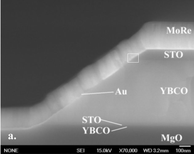
Nanostructuring of high-Tc superconducting YBCO films [1][2][3]
Nanostructuring of high-Tc YBCO films down to about 50 nm performed by ion beam milling using carbon mask. The carbon mask is structured by reactive ion beam milling using oxygen ions and, for example, a mask of HSQ e-beam resist. Remove of carbon mask and recover of superconducting properties of YBCO nanowires performed in oxygen plasma.
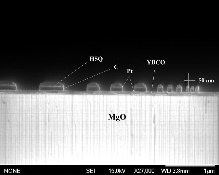

- M. I. Faley et al., Sensors vol.17(12) 2798 (2017). DOI: 10.3390/s17122798
- M. I. Faley et al., Superconductor Science and Technology vol.30 083001 (2017). DOI: 10.1088/1361-6668/aa73ad
- M. I. Faley, “Reproducible step-edge Josephson junction”, Patent US 9666783 B2 (granted 30.05.2017)
Nanostructuring of low-Tc superconducting Nb, MoRe and TiN films [1][2][3][4]
Nanostructuring of low-Tc superconducting Nb, MoRe and TiN films down to about 10 nm performed at the Helmholtz Nano Facility by reactive ion etching (RIE) using SF6 gas and, for example, a HSQ mask.
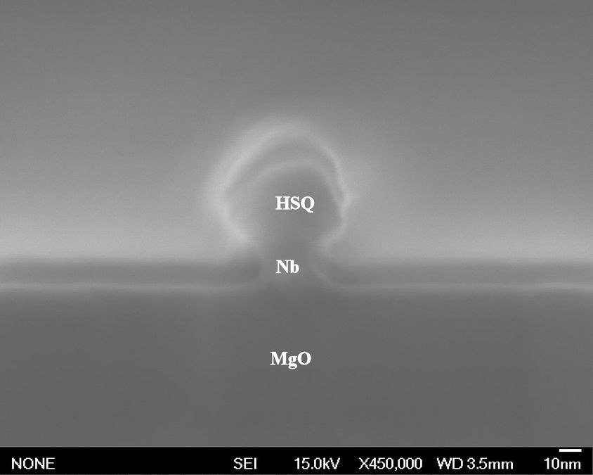
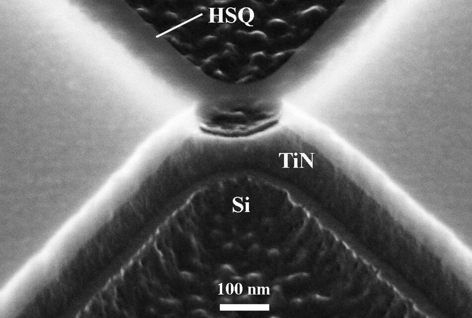
R. Rodrigo et al., Journal of Physics: Conference Series vol.1559 012011 (2020). DOI:10.1088/1742-6596/1559/1/012011
M. I. Faley et al., Superconductor Science and Technology vol.33 044005 (2020).
DOI: 10.1088/1361-6668/ab7053M. I. Faley et al., Superconductor Science and Technology vol.34 035014 (2021).
DOI: 10.1088/1361-6668/abda5cM. I. Faley et al., Nanomaterials vol. 11, 466 (2021). DOI: 10.3390/nano11020466
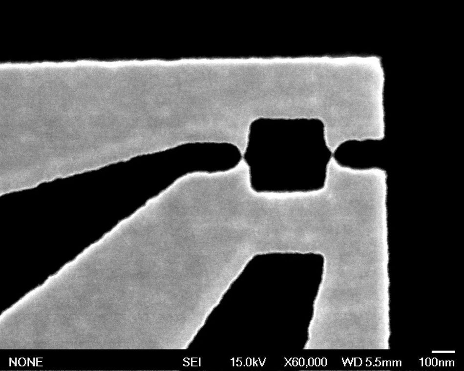
Pi-loops with Josephson junctions between d-wave and s-wave superconductors [1][2]
Josephson junctions (JJs) were prepared between the d-wave superconductor (SC) YBa2Cu3O7-x (YBCO) and the s-wave SC Nb (ds-JJs) on graphoepitaxially buffered MgO substrates, studied at temperatures down to 30 mK and used in pi-loops.
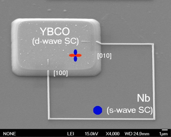
Current-voltage characteristics of ds-JJs that are oriented along the [100] axis of YBCO exhibit up to 200 times higher critical current densities than ds-JJs that are oriented along the [110] axis of YBCO. Rectangular arrays of up to 40000 pi-loops based on such ds-JJs were investigated using a low temperature scanning SQUID microscope. We observed ordering of spontaneously generated half integer magnetic flux quanta in the pi-loops. The magnetic state of the pi-loops could be manipulated by the local application of magnetic fields using nearby integrated planar coils. These results pave the way for the use of pi-loops in computations based on annealing processes.
- M. I. Faley et al., IEEE Transactions on Applied Superconductivity, vol.29 (5) 1100405 (2019). DOI: 10.1109/TASC.2019.2892078
- M. I. Faley et al., Superconductor Science and Technology vol.33 044005 (2020). DOI:10.1088/1361-6668/ab7053
π-Loops With ds Josephson Junctions
Nanofabrication and Quantum Sensing

Phone: +49 2461 61-4366
Fax: +49 2461 61-6444
E-Mail: m.faley@fz-juelich.de